| Italy’s National Metrology Institute |
The Italy’s National Metrology Institute (INRIM) is the national metrology institute of Italy with the task of carrying out and promoting scientific research in metrology, new technologies and materials. INRIM carries out studies and researches on the realisation of primary standards for the basic and derived units of the International System of units (SI), assures the maintenance of such standards, and, in addition, its main R&D areas are in fundamental physical constants, materials, nanotechnology and quantum information. Research on nanoscience and materials is carried out at INRIM from both fundamental and technological perspectives. Nanoscience explores matter behaviour on scales of the same order of atomic and molecular sizes (from 1 to 100 nanometres), where the physical properties are totally different from those on micro- and macroscopic scales, since phenomena are controlled by quantum physics. Aiming to promote new techniques in the area of metrology, sensing and imaging, unique measuring methods are investigated that can go beyond the boundaries of the classical systems using the specific characteristics of the optical quantum states, as, in particular, the correlations linked to the state of entanglement.
Website of the Italy’s National Metrology Institute: www.inrim.it
Researches involved in the SUPERGALAX project
Giorgio Brida (Gender Male) is a Senior Researcher at INRiM. He graduated in Electronic Engineering at the Politecnico di Torino in 1991, and he received the Ph.D. degree in Metrology, from the Politecnico di Torino in 1996. Since 1995 he is a staff researcher at IEN Galileo Ferraris (INRiM from 2006) where he started his activity on classical radiometry with cryogenic radiometer for the absolute spectral responsivity calibration of photodetectors. His main field of activity is the design of Silicon photodiodes with predictable spectral responsivity, the characterization of single photon detectors (SPAD, TES, SSPD e CCD) and single photon sources (SPS), parametric down-conversion in non-linear crystals and color center in diamonds. He is responsible for maintaining and disseminating the optical primary standard scale of radiant power and spectral responsivity. His current research interests includes the metrological traceability from classical radiometry to SPS, quantum enhanced measurement techniques and characterization of novel nanophotonic devices. Since 2007 he contributed as Work-Package Leader to the several European Metrology Research Project (EMRP): qu-Candela, Newstar, SIQUTE, MIQC, MIQC2 and PhotoLED.
Alice Meda (Gender Female) is a Research at INRiM. She graduated in Physics at the Università degli Studi di Torino in 2003; she received the Ph.D. degree in Metrology, from the Politecnico di Torino in 2007. Her most recent works regard, on the one side, the realization of protocols in which one of two correlated beams (twin beams or thermal light) is addressed to a target (a beam splitter or a faint object) and the other will be used as an ancilla. She applied the idea to different protocols: Sub Shot Noise quantum imaging, Ghost Imaging and dynamics of Gaussian states. On the other side, her research activity is devoted to the realization of a QKD Italian backbone for the realization of a point-to-point QKD link between Torino and Firenze and to the analysis of side channel attacks in QKD protocols.
Until March 2015, she was the principal investigator of the Torino Research Unit for the Italian three year project “FIRB 2010 -Futuro in Ricerca” Light correlations for high precision innovative sensing (LICHIS) for the design and development of innovative, high precision measurement schemes based on the correlations (classical and entanglement) existing between two or more beams of light. She has provided important contribution to European projects (QuCandela, BRISQ2, SIQUTE, MIQC, MIQC2) for quantum metrology, quantum communication and quantum information technologies.
Emanuele Enrico (Gender Male) is a Researcher at INRiM. He graduated in Physics of Advanced Technologies in 2008 (Università degli Studi di Torino). In 2012 he obtained a Ph.D. in Metrology (Politecnico di Torino). From 2010 to 2016 he has been Technical Assistant for the Research Institutions at the Italian National Institute of Metrological Research (INRiM). In the former institution he has was responsible for the realization of quantum devices based on nanostructured thin film technologies with applications in sensors, quantum metrology and the nano-photonics.
He has been guest researcher at the National Enterprise for Nanoscience and Nanotechnology (NEST) of the Scuola Normale Superiore, Pisa Italy, where he developed a reference sample device for the generation of quantized electric current. To date he is the author of 56 articles published in international journals. E.E. has been invited speaker at numerous national and international conferences, he is referee for international journals, and has been tutors of many under graduated and PhD students.
Since 2011, E.E. participates in 15 European and national projects as an expert partner in nanofabrication for thin film devices and life science. He has been workpackage leader of the “Fabrication” WP in the EMRP 2012 Microphoton project and “Impact” WP in EMPIR 2017 ParaWave. He has been PI for 3 beamline projects at the ESRF (Grenoble) and for 1 NanoSIMS (Open University, UK) project in the framework of the Europlanet 2020.
Dr. Mauro Rajteri (Gender Male) is an Electronic Engineer (Politecnico di Torino, 1990) with a PhD in Physics (Politecnico di Torino, 1996). From 1999 he is a researcher at INRIM. His main fields of research are superconducting materials and devices in particular as light detectors from UV to IR. He is responsible of the laboratory on “Innovative cryogenic devices”. During his activity, he developed skills on measurement of superconducting materials and devices at cryogenic temperatures. In the last years the research has been focalized on the development of transition-edge sensors (TESs), microcalorimeters with photon-number resolving capability operated in a 3 He/ 4 He dilution refrigerator and in an Adiabatic Demagnetization Refrigerator. He carried out activity on the optical characterization of materials (by spectrophotometry and ellipsometry) and antireflection coatings. He has been involved in research projects for the Italian Space Agency ASI on superconductive photodetectors and in many research project within the EC 7th programme ERANET-plus and EMPR. He has been the coordinator of the Piedmont Region research project E45 “Superconducting transition-edge sensors for single photon counting” (2006-2009), and “Evaluation of photon statistics with photon number resolving detectors and correlated photon pair sources” Joint Projects for the exchange of researchers within the Executive Programme Italy-Japan 2009-2012). He has been responsible of the workpackage “Optimised novel materials for high performance NEMS”, for the European project EMRP-NEW08 “Metrology with/for NEMS (MetNEMS)” (2012-2015).
He is the author of more than 70 papers on international peer reviewed journals, he is referee for international journals,
and has been tutors of many under graduated and PhD students.
Description of significant infrastructure and major items of technical equipment of the INRIM, relevant to theSUPERGALAX project
The research team has a long time experience in fabrication of thin film devices based on NV color centers, Coulombic devices, Josephson junctions and superconducting nanonwires. The research team has all necessary technological equipment for a full cycle device fabrication starting from photo mask realization up to final assembling of chips on chip carrier:
Clean room facilities;
Variable-pressure Electron Beam Lithography in a modified SEM-FIB – FEI Quanta3D FEG (beam up to 30 kV)
Laser writer system for laser beam photolithography Heidlberg uPG-101;
Chemical hoods and storages for resist preparation and development (spinner, hot-plate)
Chemical hood for lift-off processes (ultrasonic bath)
Multi-pocket (6x,4cc) high vacuum electron beam evaporator for high quality ultra-thin film (4->250 nm) deposition (normal metals and superconductors). Load-lock equipped with ion milling system (Ar, O2 – Telemark XIAD 1kV) for substrate cleaning and controlled gas inlet for tunnel junctions’ realization. Tiltable sample holder.
Ultra high vacuum dc-magnetron multi target (Nb, Al) deposition system equipped with load-look chamber.
Vacuum deposition system for thermal evaporation of metallic (Cr, Au) thin films;
Plasma Enhanced Chemical Vapour Deposition (PECVD) for the growth of SiO2 dielectric films
Reactive Ion Etching with Ar, CF4, O2 gases
Plasma Matrix (bDiscom) cleaner, N2, Ar and O2 gases for resist descum and substrate cleaning
Wedge bonder, Al wire. Bump bonding and ball bonding (Au) capabilities.
Wafer dicing: diamond scriber
Alpha Step Profilometer for thickness step-height evaluation
Ellipsometer for dielectric thickness evaluation
Optical microscope
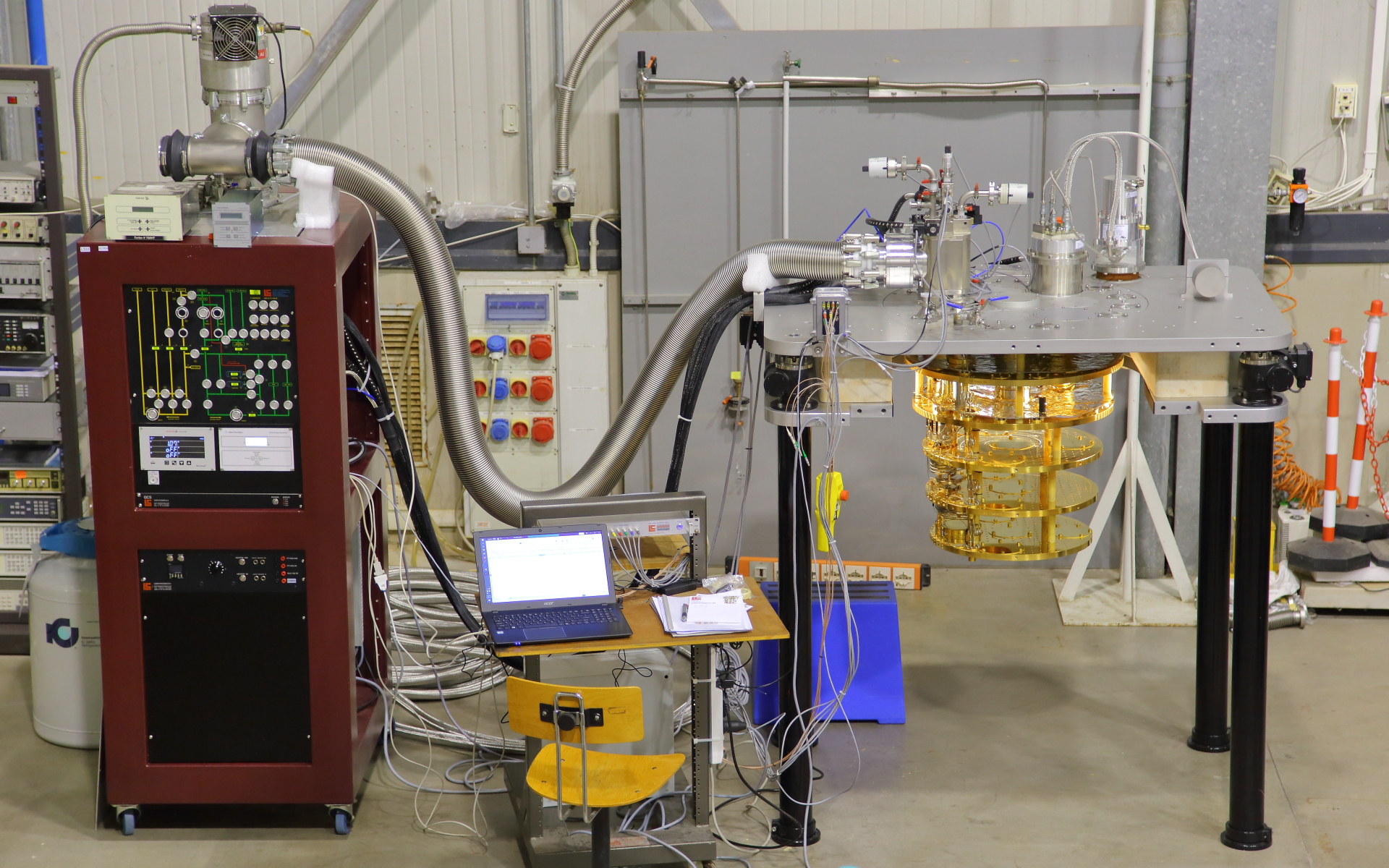
The group has an experience in experiments at ultra-low temperatures. The group is equipped by
adiabatic Demagnetization Refrigerator and Leiden Cryogenics MCK 50-100 dilution refrigerator (20 mK)
The group has the following microwave equipment:
Agilent E4440A Spectrum Analyzer (3 Hz to 26.5 GHz);
Agilent E8257D Signal generator (250 kHz to 67 GHz);
Agilent E8244A Signal generator (250 kHz – 40 GHz);
Anritsu MG3694B Signal generator 40 GHz
VNA Agilent E8364C 10 MHz – 110 GHz (in coaxial up to 50 GHz)